Applied Materials’ New Ioniq™ PVD System Solves Wiring Resistance Challenges of 2D Scaling
Chipmakers are using advances in lithography to shrink chips to the 3nm node and beyond. Unfortunately, as the wires become thinner, the electrical resistance increases exponentially, and this reduces chip performance and increases power consumption. If left unchecked, the wiring resistance can fully negate the benefits of more advanced transistors.
Chip wiring is deposited into trenches and vias that are etched into a dielectric material. In the conventional approach, the wiring is deposited using a metal stack that typically includes a barrier layer to prevent the metal from mixing with the dielectric; a liner layer to promote adhesion; a seed layer to facilitate metal fill; and a conductive metal like tungsten or cobalt for the transistor contacts and copper for the interconnect wires. The barriers and liners don’t scale well, so as the trenches and vias shrink, the proportion of space available for conductive metals is reduced; and the smaller the wiring, the higher the electrical resistance.
Applied Endura® Ioniq™ PVD System
The Ioniq PVD system is an Integrated Materials Solution™ (IMS™) that includes surface preparation along with PVD and CVD processes in a single, high-vacuum system. Ioniq PVD enables chipmakers to replace the high-resistance liner and barrier layers, typically made of titanium nitride, with a pure, low-resistance PVD tungsten film which is then combined with CVD tungsten to create a pure tungsten metal contact. The solution solves the resistance challenges and enables 2D scaling to continue to the 3nm node and beyond.
“Applied’s latest breakthrough in solving electrical resistance is a great example of how materials engineering innovations enable 2D scaling to continue,” said Dr.
The Endura Ioniq PVD system has been selected by multiple leading customers worldwide. Additional information about the system and other
About
Contact:
A photo accompanying this announcement is available at https://www.globenewswire.com/NewsRoom/AttachmentNg/50945685-c129-46ea-add1-5cd49ed1a47b
The photo is also available at Newscom, www.newscom.com, and via AP PhotoExpress.

![]()
Applied Endura® Ioniq™ PVD System
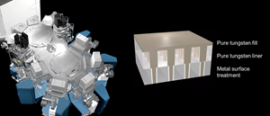
The Endura® Ioniq™ PVD system is Applied Materials’ latest breakthrough for solving wiring resistance challenges of 2D scaling. The Ioniq system is an Integrated Materials Solution™ (IMS™) that includes surface preparation along with PVD and CVD processes in a single, high-vacuum system.
Source: Applied Materials, Inc.